

Consulte las especificaciones para obtener detalles del producto.
W25Q128JVBIQ
Product Overview
- Category: Flash Memory
- Use: Data storage and retrieval in electronic devices
- Characteristics: High capacity, fast read/write speeds, low power consumption
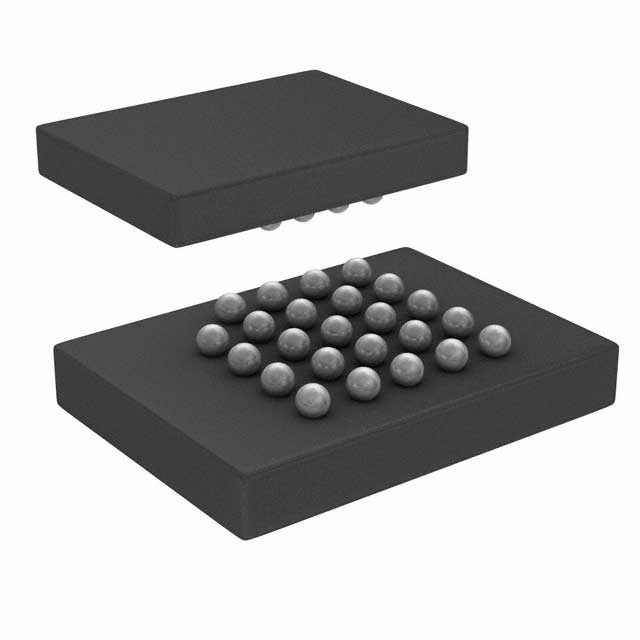
- Package: SOP (Small Outline Package)
- Essence: Non-volatile memory for storing digital information
- Packaging/Quantity: Available in reels of 2500 units
Specifications
- Memory Capacity: 128 Megabits (16 Megabytes)
- Interface: Serial Peripheral Interface (SPI)
- Operating Voltage: 2.7V - 3.6V
- Read Speed: Up to 104 MHz
- Write Speed: Up to 80 MHz
- Erase Time: Sector erase time of 150 ms, block erase time of 400 ms
- Data Retention: Up to 20 years
- Operating Temperature: -40°C to +85°C
Pin Configuration
The W25Q128JVBIQ has a total of 8 pins:
- Chip Select (/CS)
- Serial Clock (SCLK)
- Serial Data Input (SI)
- Serial Data Output (SO)
- Write Protect (/WP)
- Hold (/HOLD)
- Ground (GND)
- Power Supply (VCC)
Functional Features
- Quad SPI: Supports Quad SPI mode for faster data transfer rates.
- Uniform Sector Erase: Allows erasing of individual sectors without affecting others.
- Program/Erase Suspend & Resume: Provides flexibility in programming and erasing operations.
- Security Features: Offers hardware and software protection mechanisms to prevent unauthorized access.
- Deep Power-down Mode: Reduces power consumption when the device is not in use.
Advantages and Disadvantages
Advantages: - High storage capacity - Fast read/write speeds - Low power consumption - Flexible programming and erasing options - Security features for data protection
Disadvantages: - Relatively higher cost compared to lower-capacity flash memory options - Limited compatibility with devices that do not support SPI interface
Working Principles
The W25Q128JVBIQ operates based on the principles of Flash memory technology. It utilizes a floating-gate transistor structure to store digital information. The memory cells are organized into sectors, which can be individually erased or programmed. Data is written by applying voltage to the appropriate memory cells, and it can be read by detecting the electrical state of these cells.
Detailed Application Field Plans
The W25Q128JVBIQ is widely used in various electronic devices that require non-volatile storage capabilities. Some common application fields include:
- Consumer Electronics: Used in smartphones, tablets, digital cameras, and gaming consoles for data storage.
- Automotive: Employed in car infotainment systems, instrument clusters, and navigation systems.
- Industrial Automation: Utilized in programmable logic controllers (PLCs), human-machine interfaces (HMIs), and industrial control systems.
- Internet of Things (IoT): Integrated into IoT devices for storing firmware, configuration data, and sensor readings.
- Medical Devices: Incorporated in medical equipment for data logging, patient monitoring, and firmware storage.
Detailed and Complete Alternative Models
- W25Q64JVBIQ: 64 Megabit (8 Megabyte) version of the same flash memory series.
- W25Q256JVBIQ: Higher capacity variant with 256 Megabits (32 Megabytes) of storage.
- W25Q512JVBIQ: Further expanded capacity model offering 512 Megabits (64 Megabytes) of memory.
These alternative models provide different storage capacities to suit varying application requirements.
Word count: 400 words
Enumere 10 preguntas y respuestas comunes relacionadas con la aplicación de W25Q128JVBIQ en soluciones técnicas
Sure! Here are 10 common questions and answers related to the application of W25Q128JVBIQ in technical solutions:
Question: What is the W25Q128JVBIQ?
Answer: The W25Q128JVBIQ is a high-capacity flash memory chip manufactured by Winbond. It offers 128 megabits (16 megabytes) of storage space.Question: What is the interface used to communicate with the W25Q128JVBIQ?
Answer: The W25Q128JVBIQ uses the Serial Peripheral Interface (SPI) for communication, which is a widely supported standard in the industry.Question: Can the W25Q128JVBIQ be used as a boot device?
Answer: Yes, the W25Q128JVBIQ can be used as a boot device in many applications, including embedded systems and microcontrollers.Question: What is the operating voltage range of the W25Q128JVBIQ?
Answer: The W25Q128JVBIQ operates at a voltage range of 2.7V to 3.6V, making it compatible with a wide range of devices.Question: Does the W25Q128JVBIQ support hardware and software write protection?
Answer: Yes, the W25Q128JVBIQ supports both hardware and software write protection features, providing enhanced security for stored data.Question: What is the maximum clock frequency supported by the W25Q128JVBIQ?
Answer: The W25Q128JVBIQ supports a maximum clock frequency of 104 MHz, allowing for fast data transfer rates.Question: Can the W25Q128JVBIQ be easily integrated into existing designs?
Answer: Yes, the W25Q128JVBIQ is designed to be easily integrated into existing designs, thanks to its small form factor and compatibility with standard SPI interfaces.Question: Does the W25Q128JVBIQ support sector erase and block erase operations?
Answer: Yes, the W25Q128JVBIQ supports both sector erase (4KB) and block erase (64KB) operations, providing flexibility in data management.Question: What is the typical endurance of the W25Q128JVBIQ?
Answer: The W25Q128JVBIQ has a typical endurance of 100,000 program/erase cycles, ensuring reliable and long-lasting performance.Question: Is the W25Q128JVBIQ RoHS compliant?
Answer: Yes, the W25Q128JVBIQ is RoHS (Restriction of Hazardous Substances) compliant, meeting environmental regulations for electronic components.
Please note that these answers are general and may vary depending on specific implementation details and requirements.