

Consulte las especificaciones para obtener detalles del producto.
XC2C256-7CPG132I
Product Overview
Category
XC2C256-7CPG132I belongs to the category of programmable logic devices (PLDs).
Use
This product is commonly used in digital circuit design and implementation. It provides a flexible and customizable solution for various applications.
Characteristics
- Programmable: The XC2C256-7CPG132I can be programmed to perform specific functions, allowing for versatility in design.
- High-density: With 256 macrocells, this PLD offers a high level of integration, making it suitable for complex designs.
- Low power consumption: The device is designed to operate efficiently, minimizing power consumption.
- Fast operation: The XC2C256-7CPG132I offers high-speed performance, enabling quick execution of logic functions.
Package
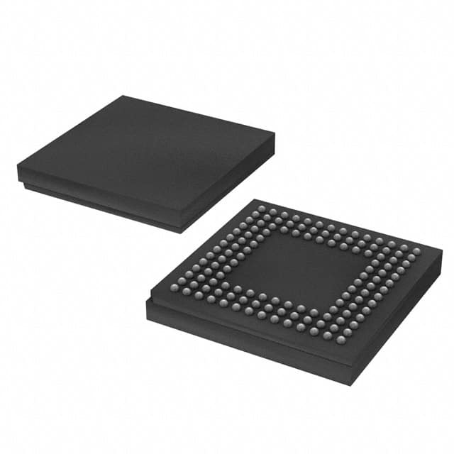
The XC2C256-7CPG132I comes in a Ceramic Pin Grid Array (CPGA) package.
Essence
The essence of XC2C256-7CPG132I lies in its ability to provide reconfigurable logic functionality, allowing designers to implement custom digital circuits without the need for dedicated hardware.
Packaging/Quantity
This product is typically packaged individually and is available in varying quantities depending on the supplier.
Specifications
- Macrocells: 256
- Logic Gates: 10,000+
- I/O Pins: 132
- Operating Voltage: 3.3V
- Speed Grade: -7
- Configuration Memory: Non-volatile Flash
Detailed Pin Configuration
The XC2C256-7CPG132I has a total of 132 pins, which are assigned different functions based on their configuration. The pinout diagram below illustrates the detailed pin configuration:

Functional Features
- Reconfigurability: The XC2C256-7CPG132I can be reprogrammed multiple times, allowing for iterative design improvements and flexibility in adapting to changing requirements.
- In-system programming: The device supports in-system programming, enabling updates to the configuration without removing it from the circuit board.
- JTAG interface: The XC2C256-7CPG132I features a Joint Test Action Group (JTAG) interface, facilitating debugging and testing during development.
Advantages and Disadvantages
Advantages
- Flexibility: The ability to reconfigure the device makes it suitable for a wide range of applications.
- Cost-effective: By eliminating the need for dedicated hardware, the XC2C256-7CPG132I reduces overall costs.
- High integration: With 256 macrocells, this PLD offers a high level of integration, reducing the need for additional components.
Disadvantages
- Learning curve: Utilizing programmable logic devices requires knowledge of hardware description languages and digital design concepts.
- Limited performance: While the XC2C256-7CPG132I provides fast operation, it may not match the performance of application-specific integrated circuits (ASICs) for certain complex designs.
Working Principles
The XC2C256-7CPG132I operates based on the principles of field-programmable gate arrays (FPGAs). It consists of configurable logic blocks (CLBs), interconnect resources, and input/output blocks (IOBs). The CLBs contain look-up tables (LUTs) that can be programmed to implement desired logic functions. The interconnect resources allow for the routing of signals between different CLBs and IOBs. The IOBs provide interfaces for external connections.
Detailed Application Field Plans
The XC2C256-7CPG132I finds applications in various fields, including:
- Communications: Used in networking equipment, routers, and switches for implementing custom protocols and interfaces.
- Industrial automation: Employed in control systems, robotics, and process automation to provide flexible and adaptable logic functionality.
- Automotive electronics: Utilized in automotive control units for implementing complex algorithms and signal processing.
- Consumer electronics: Integrated into devices such as gaming consoles, set-top boxes, and multimedia players to enable customized features and functions.
Detailed and Complete Alternative Models
- XC2C256-7VQG100C: Similar to XC2C256-7CPG132I but comes in a Quad Flat No-Lead (QFN) package with 100 pins.
- XC2C256-7FTG256C: Offers the same specifications as XC2C256-7CPG132I but comes in a Fine-Pitch Ball Grid Array (FBGA) package with 256 pins.
- XC2C256-7TQG144C: Provides the same functionality as XC2C256-7CPG132I but comes in a Thin Quad Flat Pack (TQFP) package with 144 pins.
These alternative models offer similar capabilities and can
Enumere 10 preguntas y respuestas comunes relacionadas con la aplicación de XC2C256-7CPG132I en soluciones técnicas
Sure! Here are 10 common questions and answers related to the application of XC2C256-7CPG132I in technical solutions:
Q: What is XC2C256-7CPG132I? A: XC2C256-7CPG132I is a field-programmable gate array (FPGA) manufactured by Xilinx. It offers 256 macrocells and operates at a speed grade of -7.
Q: What are the typical applications of XC2C256-7CPG132I? A: XC2C256-7CPG132I is commonly used in various technical solutions such as digital signal processing, embedded systems, communication protocols, and control systems.
Q: How can I program XC2C256-7CPG132I? A: XC2C256-7CPG132I can be programmed using Xilinx's programming tools like iMPACT or Vivado. You can use a JTAG programmer or an external PROM to configure the FPGA.
Q: What is the maximum operating frequency of XC2C256-7CPG132I? A: The maximum operating frequency of XC2C256-7CPG132I depends on the design and implementation. However, it is typically capable of operating at frequencies up to several hundred megahertz.
Q: Can XC2C256-7CPG132I interface with other components or devices? A: Yes, XC2C256-7CPG132I supports various standard interfaces like SPI, I2C, UART, and GPIOs, allowing it to communicate with other components or devices in a system.
Q: Does XC2C256-7CPG132I have built-in memory? A: No, XC2C256-7CPG132I does not have built-in memory. However, it can be used to interface with external memory devices like SRAM or DDR.
Q: What is the power supply requirement for XC2C256-7CPG132I? A: XC2C256-7CPG132I typically operates at a voltage of 3.3V, but it also supports a wide range of voltages from 1.8V to 3.6V.
Q: Can XC2C256-7CPG132I be reprogrammed multiple times? A: Yes, XC2C256-7CPG132I is a reprogrammable FPGA, which means you can program it multiple times to change its functionality or update the design.
Q: Is XC2C256-7CPG132I suitable for high-speed applications? A: Yes, XC2C256-7CPG132I is capable of handling high-speed applications due to its advanced architecture and optimized routing resources.
Q: Where can I find more information about XC2C256-7CPG132I? A: You can refer to Xilinx's official documentation, datasheets, application notes, and user guides for detailed information about XC2C256-7CPG132I and its usage in technical solutions.
Please note that the answers provided here are general and may vary depending on specific requirements and use cases.