

Consulte las especificaciones para obtener detalles del producto.
XC3S50A-5VQG100C
Product Overview
Category
The XC3S50A-5VQG100C belongs to the category of Field-Programmable Gate Arrays (FPGAs).
Use
FPGAs are integrated circuits that can be programmed and reprogrammed to perform various digital functions. The XC3S50A-5VQG100C is specifically designed for applications requiring programmable logic solutions.
Characteristics
- Programmable: The XC3S50A-5VQG100C offers flexibility as it can be configured to implement different logic functions.
- High Performance: It provides fast processing speeds and efficient execution of complex algorithms.
- Low Power Consumption: The FPGA is designed to minimize power consumption, making it suitable for battery-powered devices.
- Scalability: The XC3S50A-5VQG100C can be easily scaled up or down depending on the application requirements.
Package
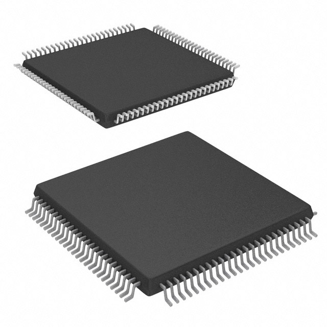
The XC3S50A-5VQG100C comes in a Quad Flat No-Lead (QFN) package.
Essence
The essence of the XC3S50A-5VQG100C lies in its ability to provide a customizable hardware solution for digital systems. It allows designers to implement specific functionalities without the need for custom-designed integrated circuits.
Packaging/Quantity
The XC3S50A-5VQG100C is typically packaged in reels and is available in quantities suitable for both prototyping and large-scale production.
Specifications
- Family: Spartan-3A
- Logic Cells: 1,152
- Flip-Flops: 2,304
- Block RAM: 36 Kbits
- Maximum Frequency: 500 MHz
- Operating Voltage: 5V
- I/O Pins: 100
Detailed Pin Configuration
The XC3S50A-5VQG100C has a total of 100 I/O pins. These pins are used for input and output connections to external devices. The pin configuration is as follows:
(Pin Number) (Pin Name) 1. VCCO 2. GND 3. IOL1PT0LN0 4. IOL1NT0LN0 5. IOL2PT0LN0 6. IOL2NT0LN0 7. IOL3PT0LN0 8. IOL3NT0LN0 9. IOL4PT0LN0 10. IOL4NT0LN0 11. IOL5PT0LN0 12. IOL5NT0LN0 13. IOL6PT0LN0 14. IOL6NT0LN0 15. IOL7PT0LN0 16. IOL7NT0LN0 17. IOL8PT0LN0 18. IOL8NT0LN0 19. IOL9PT0LN0 20. IOL9NT0LN0 21. IOL10PT0LN0 22. IOL10NT0LN0 23. IOL11PT0LN0 24. IOL11NT0LN0 25. IOL12PT0LN0 26. IOL12NT0LN0 27. IOL13PT0LN0 28. IOL13NT0LN0 29. IOL14PT0LN0 30. IOL14NT0LN0 31. IOL15PT0LN0 32. IOL15NT0LN0 33. IOL16PT0LN0 34. IOL16NT0LN0 35. IOL17PT0LN0 36. IOL17NT0LN0 37. IOL18PT0LN0 38. IOL18NT0LN0 39. IOL19PT0LN0 40. IOL19NT0LN0 41. IOL20PT0LN0 42. IOL20NT0LN0 43. IOL21PT0LN0 44. IOL21NT0LN0 45. IOL22PT0
Enumere 10 preguntas y respuestas comunes relacionadas con la aplicación de XC3S50A-5VQG100C en soluciones técnicas
Sure! Here are 10 common questions and answers related to the application of XC3S50A-5VQG100C in technical solutions:
Question: What is XC3S50A-5VQG100C?
Answer: XC3S50A-5VQG100C is a specific model of Field-Programmable Gate Array (FPGA) manufactured by Xilinx.Question: What are the key features of XC3S50A-5VQG100C?
Answer: Some key features include 50,000 system gates, 36Kbits of block RAM, 4 Digital Clock Managers (DCMs), and support for various I/O standards.Question: What are the typical applications of XC3S50A-5VQG100C?
Answer: XC3S50A-5VQG100C is commonly used in applications such as digital signal processing, embedded systems, communication systems, and industrial automation.Question: How can XC3S50A-5VQG100C be programmed?
Answer: XC3S50A-5VQG100C can be programmed using Xilinx's Vivado Design Suite or ISE Design Suite software tools.Question: What voltage level does XC3S50A-5VQG100C operate at?
Answer: XC3S50A-5VQG100C operates at a voltage level of 5V.Question: Can XC3S50A-5VQG100C be used in low-power applications?
Answer: No, XC3S50A-5VQG100C is not suitable for low-power applications as it operates at a higher voltage level.Question: What is the maximum clock frequency supported by XC3S50A-5VQG100C?
Answer: The maximum clock frequency supported by XC3S50A-5VQG100C is typically around 200 MHz.Question: Can XC3S50A-5VQG100C be used for high-speed data processing?
Answer: Yes, XC3S50A-5VQG100C can handle high-speed data processing due to its efficient architecture and support for advanced features like DCMs.Question: Are there any specific design considerations when using XC3S50A-5VQG100C?
Answer: Yes, designers should consider factors such as power supply requirements, I/O voltage compatibility, and thermal management while designing with XC3S50A-5VQG100C.Question: Is XC3S50A-5VQG100C a cost-effective FPGA option?
Answer: Yes, XC3S50A-5VQG100C is considered a cost-effective FPGA option due to its reasonable price point and versatile capabilities.
Please note that the answers provided here are general and may vary depending on specific application requirements and design considerations.