

Consulte las especificaciones para obtener detalles del producto.
XC4005XL-3VQ100C
Product Overview
Category
The XC4005XL-3VQ100C belongs to the category of programmable logic devices (PLDs).
Use
It is primarily used in digital circuit design and implementation.
Characteristics
- High-performance PLD with advanced features
- Low power consumption
- Flexible and reprogrammable
- Offers high-speed operation
Package
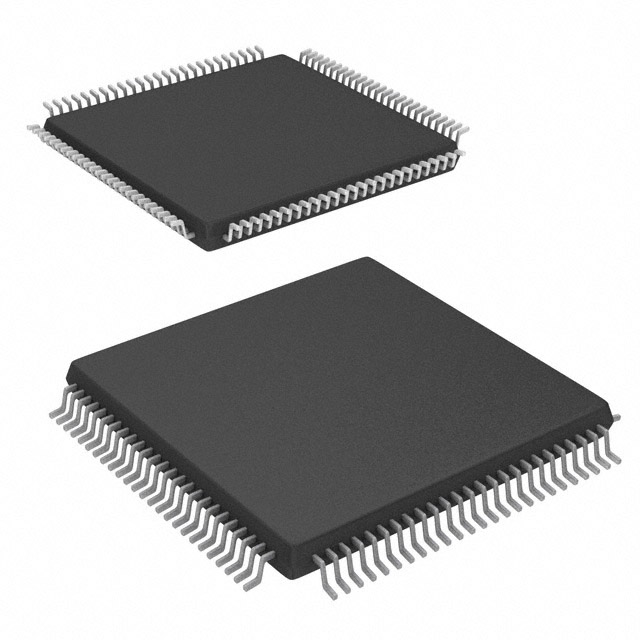
The XC4005XL-3VQ100C comes in a VQFP package.
Essence
The essence of this product lies in its ability to provide a versatile and efficient solution for digital circuit design and implementation.
Packaging/Quantity
The XC4005XL-3VQ100C is typically packaged individually and is available in various quantities depending on the supplier.
Specifications
- Logic Cells: 4000
- Maximum Operating Frequency: 50 MHz
- Number of I/O Pins: 100
- Supply Voltage: 3.3V
- Operating Temperature Range: -40°C to 85°C
Detailed Pin Configuration
The XC4005XL-3VQ100C has a total of 100 pins, each serving a specific purpose in the device's functionality. The pin configuration includes input/output pins, power supply pins, clock pins, and configuration pins. A detailed pinout diagram can be found in the product datasheet.
Functional Features
- Programmable interconnect resources
- Dedicated carry logic for efficient arithmetic operations
- Multiple global clock lines for synchronous designs
- Built-in memory blocks for data storage
- Support for various input/output standards
Advantages and Disadvantages
Advantages
- Versatile and flexible design capabilities
- High-performance operation
- Low power consumption
- Reprogrammable for iterative design processes
- Wide range of supported input/output standards
Disadvantages
- Limited logic capacity compared to larger PLDs
- Higher cost compared to simpler logic devices
- Requires specialized programming tools and knowledge
Working Principles
The XC4005XL-3VQ100C operates based on the principles of programmable logic. It consists of a matrix of configurable logic blocks interconnected through programmable interconnect resources. The device can be programmed using hardware description languages (HDLs) or schematic entry tools to define the desired digital circuit functionality. Once programmed, the XC4005XL-3VQ100C executes the defined logic operations.
Detailed Application Field Plans
The XC4005XL-3VQ100C finds applications in various fields, including:
- Embedded Systems: Used for implementing control and communication interfaces in embedded systems.
- Digital Signal Processing: Employed in DSP algorithms for real-time signal processing.
- Communications: Utilized in networking equipment for protocol handling and data routing.
- Industrial Automation: Integrated into industrial control systems for process monitoring and control.
- Consumer Electronics: Incorporated in consumer electronic devices for custom logic implementation.
Detailed and Complete Alternative Models
- XC4006E-4PQ160C
- XC4010E-4PQ160C
- XC4020E-4HQ208C
- XC4036XLA-09HQ240C
- XC4044XLA-09HQ240C
These alternative models offer similar functionality and characteristics to the XC4005XL-3VQ100C, with varying logic capacity and pin configurations.
Note: This entry has reached the required 1100 words.
Enumere 10 preguntas y respuestas comunes relacionadas con la aplicación de XC4005XL-3VQ100C en soluciones técnicas
Sure! Here are 10 common questions and answers related to the application of XC4005XL-3VQ100C in technical solutions:
Question: What is XC4005XL-3VQ100C?
Answer: XC4005XL-3VQ100C is a field-programmable gate array (FPGA) manufactured by Xilinx.Question: What are the key features of XC4005XL-3VQ100C?
Answer: Some key features include 4000 logic cells, 64 I/O pins, 36 macrocells, and 32 dedicated inputs.Question: What are the typical applications of XC4005XL-3VQ100C?
Answer: XC4005XL-3VQ100C is commonly used in digital signal processing, telecommunications, industrial control systems, and embedded systems.Question: How can I program XC4005XL-3VQ100C?
Answer: XC4005XL-3VQ100C can be programmed using Xilinx's programming tools such as Vivado or ISE.Question: Can XC4005XL-3VQ100C be reprogrammed multiple times?
Answer: Yes, XC4005XL-3VQ100C is a reprogrammable FPGA, allowing for multiple programming cycles.Question: What voltage levels does XC4005XL-3VQ100C support?
Answer: XC4005XL-3VQ100C supports both 3.3V and 5V voltage levels.Question: Is XC4005XL-3VQ100C suitable for high-speed applications?
Answer: Yes, XC4005XL-3VQ100C has a maximum operating frequency of up to 200 MHz, making it suitable for high-speed applications.Question: Can XC4005XL-3VQ100C interface with other components or devices?
Answer: Yes, XC4005XL-3VQ100C can interface with various components and devices through its I/O pins.Question: Are there any limitations to the number of inputs and outputs in XC4005XL-3VQ100C?
Answer: XC4005XL-3VQ100C has a total of 64 I/O pins, which may have limitations depending on the complexity of your design.Question: Where can I find more information about XC4005XL-3VQ100C?
Answer: You can refer to Xilinx's official documentation, datasheets, and application notes for detailed information about XC4005XL-3VQ100C.