

Consulte las especificaciones para obtener detalles del producto.
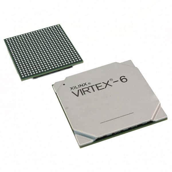
XC6VLX365T-2FFG1759C
Product Overview
Category
The XC6VLX365T-2FFG1759C belongs to the category of Field Programmable Gate Arrays (FPGAs).
Use
FPGAs are integrated circuits that can be programmed after manufacturing, allowing for flexible and customizable digital logic designs. The XC6VLX365T-2FFG1759C is specifically designed for high-performance applications.
Characteristics
- High-performance FPGA with advanced features
- Large capacity and high-speed processing capabilities
- Flexible and reconfigurable design
- Suitable for complex digital logic designs
- Optimized for high-speed data processing
Package
The XC6VLX365T-2FFG1759C comes in a Flip Chip FineLine BGA package.
Essence
The essence of the XC6VLX365T-2FFG1759C lies in its ability to provide a highly configurable and powerful platform for implementing complex digital logic designs.
Packaging/Quantity
The XC6VLX365T-2FFG1759C is typically sold individually or in small quantities, depending on the supplier.
Specifications
- Logic Cells: 362,080
- CLB Flip-Flops: 724,160
- Block RAM: 4,860 Kb
- DSP Slices: 1,920
- Maximum I/O Pins: 1,759
- Operating Voltage: 1.0V - 1.2V
- Operating Temperature: -40°C to +100°C
- Package Type: Flip Chip FineLine BGA
- Package Pins: 1759
Detailed Pin Configuration
The detailed pin configuration of the XC6VLX365T-2FFG1759C can be found in the manufacturer's datasheet.
Functional Features
- High-performance processing capabilities
- Configurable logic cells for implementing complex designs
- Dedicated DSP slices for efficient signal processing
- Flexible I/O options for interfacing with external devices
- On-chip memory blocks for data storage and retrieval
- Clock management resources for precise timing control
Advantages and Disadvantages
Advantages
- High capacity and performance for demanding applications
- Flexibility to reconfigure the FPGA as per design requirements
- Efficient utilization of resources for optimized designs
- Support for various communication protocols and interfaces
- Availability of development tools and libraries for ease of implementation
Disadvantages
- Steep learning curve for beginners due to the complexity of FPGA programming
- Higher power consumption compared to other programmable logic devices
- Relatively higher cost compared to traditional microcontrollers or ASICs
- Limited availability of alternative models with similar specifications
Working Principles
The XC6VLX365T-2FFG1759C operates based on the principles of configurable logic and interconnectivity. It consists of a large number of configurable logic cells, memory blocks, and dedicated DSP slices interconnected through programmable routing resources. The user can program the FPGA using hardware description languages (HDL) such as VHDL or Verilog to define the desired digital logic functionality. Once programmed, the FPGA executes the logic operations based on the input signals and produces the desired output.
Detailed Application Field Plans
The XC6VLX365T-2FFG1759C finds applications in various fields, including:
- Telecommunications: Used in high-speed data transmission systems, network routers, and switches.
- Aerospace and Defense: Employed in radar systems, avionics, and secure communication equipment.
- Industrial Automation: Utilized in control systems, robotics, and machine vision applications.
- Medical Devices: Integrated into medical imaging systems, patient monitoring devices, and diagnostic equipment.
- Research and Development: Used in prototyping and development of custom digital logic designs.
Detailed and Complete Alternative Models
- XC6VLX240T-2FFG1156C
- XC6VLX550T-2FFG1759C
- XC6VLX130T-2FFG1156C
- XC6VLX365T-1FFG1156C
- XC6VLX760T-2FFG1760C
These alternative models offer varying capacities, performance levels, and package options to cater to different design requirements.
Note: The above information is based on the available data at the time of writing and may be subject to change. It is recommended to refer to the manufacturer's documentation for the most up-to-date and accurate information.
Enumere 10 preguntas y respuestas comunes relacionadas con la aplicación de XC6VLX365T-2FFG1759C en soluciones técnicas
Sure! Here are 10 common questions and answers related to the application of XC6VLX365T-2FFG1759C in technical solutions:
Question: What is XC6VLX365T-2FFG1759C?
- Answer: XC6VLX365T-2FFG1759C is a specific model of Xilinx Virtex-6 FPGA (Field-Programmable Gate Array) that offers high-performance processing capabilities for various technical applications.Question: What are the key features of XC6VLX365T-2FFG1759C?
- Answer: Some key features of XC6VLX365T-2FFG1759C include a large number of logic cells, high-speed serial transceivers, embedded memory blocks, DSP slices, and support for various communication protocols.Question: In what technical solutions can XC6VLX365T-2FFG1759C be used?
- Answer: XC6VLX365T-2FFG1759C can be used in a wide range of technical solutions such as aerospace and defense systems, telecommunications equipment, industrial automation, medical devices, and high-performance computing.Question: How does XC6VLX365T-2FFG1759C enhance system performance?
- Answer: XC6VLX365T-2FFG1759C enhances system performance by providing high-speed data processing, parallel execution of tasks, and efficient utilization of hardware resources through its programmable logic fabric.Question: Can XC6VLX365T-2FFG1759C be reprogrammed after deployment?
- Answer: Yes, XC6VLX365T-2FFG1759C is a field-programmable device, which means it can be reprogrammed even after it has been deployed in a system, allowing for flexibility and adaptability.Question: What tools are available for programming XC6VLX365T-2FFG1759C?
- Answer: Xilinx provides various software tools like Vivado Design Suite and ISE Design Suite that enable users to design, simulate, and program XC6VLX365T-2FFG1759C.Question: How can XC6VLX365T-2FFG1759C be interfaced with other components?
- Answer: XC6VLX365T-2FFG1759C supports various communication protocols such as PCIe, Ethernet, USB, and high-speed serial interfaces, making it compatible with a wide range of external components.Question: What are the power requirements for XC6VLX365T-2FFG1759C?
- Answer: The power requirements for XC6VLX365T-2FFG1759C depend on the specific implementation and configuration. It is important to refer to the datasheet and design guidelines provided by Xilinx for accurate power estimation.Question: Are there any limitations or considerations when using XC6VLX365T-2FFG1759C?
- Answer: Some considerations include thermal management due to high power consumption, proper signal integrity design for high-speed interfaces, and understanding the limitations of the FPGA's resources and performance.Question: Where can I find more information about XC6VLX365T-2FFG1759C?
- Answer: You can find more detailed information about XC6VLX365T-2FFG1759C, including datasheets, application notes, and user guides, on the official Xilinx website or by contacting their technical support team.